1. Crystal Framework and Polytypism of Silicon Carbide
1.1 Cubic and Hexagonal Polytypes: From 3C to 6H and Past
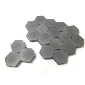
(Silicon Carbide Ceramics)
Silicon carbide (SiC) is a covalently bonded ceramic made up of silicon and carbon atoms arranged in a tetrahedral sychronisation, forming one of one of the most intricate systems of polytypism in products scientific research.
Unlike a lot of ceramics with a single steady crystal structure, SiC exists in over 250 well-known polytypes– distinct stacking series of close-packed Si-C bilayers along the c-axis– ranging from cubic 3C-SiC (likewise referred to as β-SiC) to hexagonal 6H-SiC and rhombohedral 15R-SiC.
One of the most usual polytypes made use of in engineering applications are 3C (cubic), 4H, and 6H (both hexagonal), each displaying slightly different digital band structures and thermal conductivities.
3C-SiC, with its zinc blende framework, has the narrowest bandgap (~ 2.3 eV) and is normally grown on silicon substratums for semiconductor gadgets, while 4H-SiC uses exceptional electron movement and is liked for high-power electronics.
The strong covalent bonding and directional nature of the Si– C bond provide remarkable solidity, thermal stability, and resistance to sneak and chemical attack, making SiC perfect for extreme environment applications.
1.2 Defects, Doping, and Electronic Feature
Despite its structural intricacy, SiC can be doped to attain both n-type and p-type conductivity, allowing its use in semiconductor devices.
Nitrogen and phosphorus serve as donor impurities, introducing electrons into the transmission band, while light weight aluminum and boron work as acceptors, producing holes in the valence band.
However, p-type doping effectiveness is restricted by high activation powers, especially in 4H-SiC, which presents challenges for bipolar tool style.
Native issues such as screw misplacements, micropipes, and piling faults can deteriorate device performance by acting as recombination centers or leakage paths, demanding premium single-crystal growth for electronic applications.
The broad bandgap (2.3– 3.3 eV depending on polytype), high failure electrical area (~ 3 MV/cm), and superb thermal conductivity (~ 3– 4 W/m · K for 4H-SiC) make SiC far superior to silicon in high-temperature, high-voltage, and high-frequency power electronics.
2. Handling and Microstructural Engineering
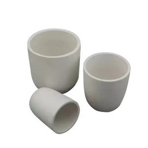
( Silicon Carbide Ceramics)
2.1 Sintering and Densification Techniques
Silicon carbide is inherently hard to densify because of its solid covalent bonding and low self-diffusion coefficients, calling for advanced handling methods to achieve full density without ingredients or with marginal sintering help.
Pressureless sintering of submicron SiC powders is feasible with the enhancement of boron and carbon, which advertise densification by removing oxide layers and enhancing solid-state diffusion.
Hot pushing uses uniaxial stress during home heating, allowing complete densification at lower temperature levels (~ 1800– 2000 ° C )and generating fine-grained, high-strength components appropriate for reducing tools and use components.
For big or complex shapes, reaction bonding is utilized, where porous carbon preforms are penetrated with molten silicon at ~ 1600 ° C, creating β-SiC sitting with minimal contraction.
Nevertheless, recurring totally free silicon (~ 5– 10%) remains in the microstructure, restricting high-temperature efficiency and oxidation resistance over 1300 ° C.
2.2 Additive Manufacturing and Near-Net-Shape Manufacture
Current advances in additive production (AM), particularly binder jetting and stereolithography utilizing SiC powders or preceramic polymers, allow the manufacture of complex geometries formerly unattainable with traditional methods.
In polymer-derived ceramic (PDC) paths, fluid SiC precursors are formed via 3D printing and afterwards pyrolyzed at high temperatures to generate amorphous or nanocrystalline SiC, often needing more densification.
These methods lower machining expenses and product waste, making SiC much more accessible for aerospace, nuclear, and warm exchanger applications where complex styles boost efficiency.
Post-processing actions such as chemical vapor seepage (CVI) or fluid silicon infiltration (LSI) are sometimes used to boost density and mechanical stability.
3. Mechanical, Thermal, and Environmental Performance
3.1 Strength, Hardness, and Put On Resistance
Silicon carbide rates among the hardest well-known products, with a Mohs hardness of ~ 9.5 and Vickers firmness exceeding 25 Grade point average, making it highly immune to abrasion, erosion, and scratching.
Its flexural toughness normally varies from 300 to 600 MPa, relying on handling approach and grain size, and it maintains strength at temperatures as much as 1400 ° C in inert environments.
Fracture strength, while moderate (~ 3– 4 MPa · m ¹/ TWO), is sufficient for many architectural applications, specifically when integrated with fiber support in ceramic matrix composites (CMCs).
SiC-based CMCs are used in wind turbine blades, combustor linings, and brake systems, where they offer weight financial savings, fuel efficiency, and extended life span over metallic equivalents.
Its superb wear resistance makes SiC perfect for seals, bearings, pump elements, and ballistic shield, where durability under severe mechanical loading is crucial.
3.2 Thermal Conductivity and Oxidation Stability
One of SiC’s most useful residential or commercial properties is its high thermal conductivity– approximately 490 W/m · K for single-crystal 4H-SiC and ~ 30– 120 W/m · K for polycrystalline forms– going beyond that of several metals and allowing reliable warm dissipation.
This property is important in power electronics, where SiC tools generate less waste heat and can run at greater power thickness than silicon-based gadgets.
At raised temperature levels in oxidizing settings, SiC develops a protective silica (SiO ₂) layer that slows down further oxidation, supplying excellent ecological toughness approximately ~ 1600 ° C.
Nonetheless, in water vapor-rich atmospheres, this layer can volatilize as Si(OH)₄, bring about accelerated destruction– a vital difficulty in gas wind turbine applications.
4. Advanced Applications in Power, Electronics, and Aerospace
4.1 Power Electronic Devices and Semiconductor Gadgets
Silicon carbide has transformed power electronics by allowing devices such as Schottky diodes, MOSFETs, and JFETs that operate at higher voltages, regularities, and temperatures than silicon matchings.
These gadgets reduce power losses in electric automobiles, renewable resource inverters, and industrial electric motor drives, adding to worldwide power effectiveness improvements.
The ability to operate at joint temperatures above 200 ° C permits simplified cooling systems and enhanced system reliability.
Additionally, SiC wafers are made use of as substrates for gallium nitride (GaN) epitaxy in high-electron-mobility transistors (HEMTs), incorporating the benefits of both wide-bandgap semiconductors.
4.2 Nuclear, Aerospace, and Optical Equipments
In nuclear reactors, SiC is an essential element of accident-tolerant fuel cladding, where its reduced neutron absorption cross-section, radiation resistance, and high-temperature stamina boost security and efficiency.
In aerospace, SiC fiber-reinforced composites are made use of in jet engines and hypersonic automobiles for their lightweight and thermal stability.
Additionally, ultra-smooth SiC mirrors are employed in space telescopes due to their high stiffness-to-density ratio, thermal stability, and polishability to sub-nanometer roughness.
In recap, silicon carbide porcelains represent a cornerstone of modern-day innovative materials, combining remarkable mechanical, thermal, and digital residential or commercial properties.
Via exact control of polytype, microstructure, and processing, SiC continues to allow technical innovations in power, transportation, and extreme setting design.
5. Provider
TRUNNANO is a supplier of Spherical Tungsten Powder with over 12 years of experience in nano-building energy conservation and nanotechnology development. It accepts payment via Credit Card, T/T, West Union and Paypal. Trunnano will ship the goods to customers overseas through FedEx, DHL, by air, or by sea. If you want to know more about Spherical Tungsten Powder, please feel free to contact us and send an inquiry(sales5@nanotrun.com).
Tags: silicon carbide ceramic,silicon carbide ceramic products, industry ceramic
All articles and pictures are from the Internet. If there are any copyright issues, please contact us in time to delete.
Inquiry us