1. Crystal Structure and Layered Anisotropy
1.1 The 2H and 1T Polymorphs: Architectural and Electronic Duality
(Molybdenum Disulfide)
Molybdenum disulfide (MoS ₂) is a split shift steel dichalcogenide (TMD) with a chemical formula consisting of one molybdenum atom sandwiched between 2 sulfur atoms in a trigonal prismatic coordination, developing covalently bonded S– Mo– S sheets.
These individual monolayers are piled vertically and held with each other by weak van der Waals forces, allowing simple interlayer shear and exfoliation down to atomically slim two-dimensional (2D) crystals– a structural feature main to its diverse functional duties.
MoS ₂ exists in several polymorphic types, one of the most thermodynamically steady being the semiconducting 2H stage (hexagonal proportion), where each layer displays a straight bandgap of ~ 1.8 eV in monolayer form that transitions to an indirect bandgap (~ 1.3 eV) wholesale, a phenomenon critical for optoelectronic applications.
In contrast, the metastable 1T stage (tetragonal symmetry) takes on an octahedral coordination and behaves as a metal conductor due to electron contribution from the sulfur atoms, making it possible for applications in electrocatalysis and conductive compounds.
Phase changes between 2H and 1T can be induced chemically, electrochemically, or via stress engineering, providing a tunable platform for creating multifunctional gadgets.
The capacity to stabilize and pattern these stages spatially within a single flake opens up paths for in-plane heterostructures with unique digital domain names.
1.2 Problems, Doping, and Edge States
The performance of MoS two in catalytic and digital applications is highly sensitive to atomic-scale problems and dopants.
Inherent point problems such as sulfur vacancies act as electron contributors, enhancing n-type conductivity and serving as active websites for hydrogen development responses (HER) in water splitting.
Grain limits and line problems can either impede fee transport or create local conductive paths, depending on their atomic setup.
Controlled doping with transition steels (e.g., Re, Nb) or chalcogens (e.g., Se) allows fine-tuning of the band framework, service provider focus, and spin-orbit coupling results.
Notably, the edges of MoS two nanosheets, particularly the metal Mo-terminated (10– 10) sides, display significantly greater catalytic activity than the inert basal aircraft, motivating the design of nanostructured drivers with taken full advantage of edge direct exposure.
( Molybdenum Disulfide)
These defect-engineered systems exemplify just how atomic-level adjustment can change a normally taking place mineral into a high-performance practical product.
2. Synthesis and Nanofabrication Techniques
2.1 Mass and Thin-Film Manufacturing Methods
Natural molybdenite, the mineral form of MoS TWO, has actually been utilized for years as a solid lubricant, yet modern applications demand high-purity, structurally managed artificial forms.
Chemical vapor deposition (CVD) is the dominant method for generating large-area, high-crystallinity monolayer and few-layer MoS two movies on substratums such as SiO ₂/ Si, sapphire, or versatile polymers.
In CVD, molybdenum and sulfur forerunners (e.g., MoO ₃ and S powder) are vaporized at heats (700– 1000 ° C )controlled atmospheres, enabling layer-by-layer growth with tunable domain name dimension and orientation.
Mechanical peeling (“scotch tape technique”) continues to be a standard for research-grade samples, yielding ultra-clean monolayers with minimal defects, though it does not have scalability.
Liquid-phase peeling, entailing sonication or shear mixing of mass crystals in solvents or surfactant services, produces colloidal dispersions of few-layer nanosheets suitable for finishings, composites, and ink solutions.
2.2 Heterostructure Integration and Gadget Pattern
The true capacity of MoS two emerges when incorporated right into vertical or side heterostructures with other 2D products such as graphene, hexagonal boron nitride (h-BN), or WSe two.
These van der Waals heterostructures enable the style of atomically specific tools, consisting of tunneling transistors, photodetectors, and light-emitting diodes (LEDs), where interlayer fee and energy transfer can be engineered.
Lithographic pattern and etching techniques permit the construction of nanoribbons, quantum dots, and field-effect transistors (FETs) with channel lengths to 10s of nanometers.
Dielectric encapsulation with h-BN secures MoS ₂ from environmental deterioration and lowers cost scattering, dramatically enhancing carrier mobility and tool security.
These manufacture developments are important for transitioning MoS ₂ from lab inquisitiveness to viable component in next-generation nanoelectronics.
3. Useful Features and Physical Mechanisms
3.1 Tribological Actions and Strong Lubrication
Among the oldest and most enduring applications of MoS ₂ is as a completely dry strong lube in severe atmospheres where fluid oils fail– such as vacuum, high temperatures, or cryogenic conditions.
The reduced interlayer shear stamina of the van der Waals gap allows very easy moving between S– Mo– S layers, resulting in a coefficient of friction as reduced as 0.03– 0.06 under optimum conditions.
Its performance is better improved by strong attachment to metal surface areas and resistance to oxidation up to ~ 350 ° C in air, past which MoO ₃ formation enhances wear.
MoS ₂ is extensively used in aerospace systems, vacuum pumps, and weapon elements, usually applied as a covering via burnishing, sputtering, or composite incorporation right into polymer matrices.
Recent studies reveal that moisture can deteriorate lubricity by boosting interlayer attachment, triggering research study right into hydrophobic coatings or hybrid lubricating substances for improved environmental security.
3.2 Electronic and Optoelectronic Reaction
As a direct-gap semiconductor in monolayer form, MoS two exhibits strong light-matter interaction, with absorption coefficients exceeding 10 ⁵ centimeters ⁻¹ and high quantum yield in photoluminescence.
This makes it ideal for ultrathin photodetectors with fast action times and broadband sensitivity, from noticeable to near-infrared wavelengths.
Field-effect transistors based on monolayer MoS ₂ show on/off proportions > 10 ⁸ and service provider flexibilities as much as 500 centimeters TWO/ V · s in suspended examples, though substrate communications normally limit functional worths to 1– 20 cm ²/ V · s.
Spin-valley combining, an effect of strong spin-orbit interaction and damaged inversion proportion, enables valleytronics– an unique standard for details encoding making use of the valley degree of freedom in momentum room.
These quantum sensations position MoS two as a prospect for low-power logic, memory, and quantum computer aspects.
4. Applications in Power, Catalysis, and Arising Technologies
4.1 Electrocatalysis for Hydrogen Development Reaction (HER)
MoS ₂ has emerged as an encouraging non-precious alternative to platinum in the hydrogen evolution response (HER), a crucial procedure in water electrolysis for environment-friendly hydrogen production.
While the basic aircraft is catalytically inert, side sites and sulfur jobs display near-optimal hydrogen adsorption totally free power (ΔG_H * ≈ 0), equivalent to Pt.
Nanostructuring techniques– such as producing up and down lined up nanosheets, defect-rich movies, or drugged crossbreeds with Ni or Co– make best use of active website thickness and electric conductivity.
When incorporated right into electrodes with conductive sustains like carbon nanotubes or graphene, MoS two accomplishes high current thickness and long-term stability under acidic or neutral problems.
Additional enhancement is achieved by supporting the metallic 1T stage, which boosts intrinsic conductivity and exposes added active websites.
4.2 Versatile Electronics, Sensors, and Quantum Instruments
The mechanical adaptability, transparency, and high surface-to-volume proportion of MoS two make it optimal for adaptable and wearable electronic devices.
Transistors, reasoning circuits, and memory devices have actually been shown on plastic substrates, making it possible for bendable screens, health screens, and IoT sensors.
MoS ₂-based gas sensors display high sensitivity to NO ₂, NH THREE, and H TWO O as a result of charge transfer upon molecular adsorption, with reaction times in the sub-second variety.
In quantum innovations, MoS ₂ hosts localized excitons and trions at cryogenic temperatures, and strain-induced pseudomagnetic fields can catch providers, enabling single-photon emitters and quantum dots.
These developments highlight MoS ₂ not only as a practical product but as a platform for exploring fundamental physics in minimized measurements.
In recap, molybdenum disulfide exhibits the convergence of classical products scientific research and quantum design.
From its ancient duty as a lubricating substance to its contemporary deployment in atomically slim electronic devices and energy systems, MoS ₂ remains to redefine the boundaries of what is feasible in nanoscale materials design.
As synthesis, characterization, and integration methods advance, its influence throughout science and modern technology is poised to expand also better.
5. Vendor
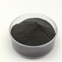
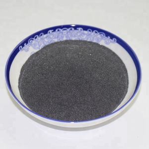
TRUNNANO is a globally recognized Molybdenum Disulfide manufacturer and supplier of compounds with more than 12 years of expertise in the highest quality nanomaterials and other chemicals. The company develops a variety of powder materials and chemicals. Provide OEM service. If you need high quality Molybdenum Disulfide, please feel free to contact us. You can click on the product to contact us.
Tags: Molybdenum Disulfide, nano molybdenum disulfide, MoS2
All articles and pictures are from the Internet. If there are any copyright issues, please contact us in time to delete.
Inquiry us